| CPC H01L 29/7851 (2013.01) [H01L 21/02532 (2013.01); H01L 21/02546 (2013.01); H01L 21/02603 (2013.01); H01L 27/0886 (2013.01); H01L 29/0653 (2013.01); H01L 29/0673 (2013.01); H01L 29/0847 (2013.01); H01L 29/161 (2013.01); H01L 29/41733 (2013.01); H01L 29/41791 (2013.01); H01L 29/42392 (2013.01); H01L 29/66439 (2013.01); H01L 29/66522 (2013.01); H01L 29/66545 (2013.01); H01L 29/66742 (2013.01); H01L 29/66795 (2013.01); H01L 29/775 (2013.01); H01L 29/78618 (2013.01); H01L 29/78684 (2013.01); H01L 29/78696 (2013.01)] | 20 Claims |
|
1. An integrated circuit (IC) comprising:
a nanostructure of semiconductor material including at least 70% germanium by atomic percentage;
a gate structure completely surrounding the nanostructure, the gate structure including a gate dielectric and a gate electrode;
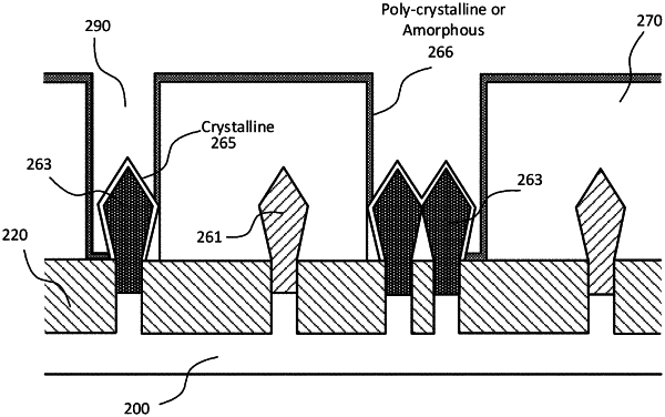
a source region and a drain region both adjacent to the nanostructure such that the nanostructure is between the source and drain regions, the source region and the drain region comprising a semiconductor material comprising silicon, and at least one of the source region and the drain region including n-type impurity;
a contact structure on the at least one of the source region and the drain region; and
a layer of mono-crystalline semiconductor material distinct from and between the at least one of the source region and the drain region and the contact structure, the layer of mono-crystalline semiconductor material comprising the semiconductor material comprising silicon, and the mono-crystalline semiconductor material including the n-type impurity.
|