| CPC H01L 29/6656 (2013.01) [G01N 27/4145 (2013.01)] | 20 Claims |
|
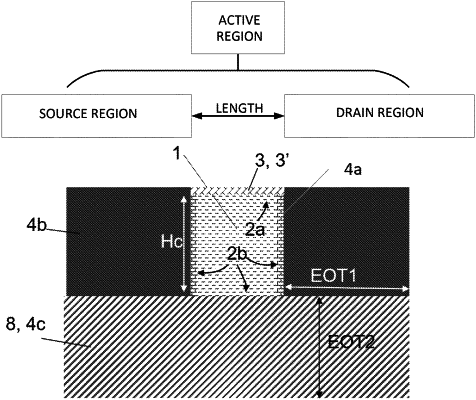
1. A method for forming a sensor, the method comprising:
providing an active region comprising a source region, a drain region, and a semiconductor channel region between the source region and the drain region, the semiconductor channel region having:
a length, and
a periphery consisting of one or more surfaces having said length, said periphery comprising a first part and a second part, the second part being different from the first part, each part having said length, the first part representing from 10 to 75% of an area of the periphery and the second part representing from 25 to 90% of the area of the periphery;
providing a first dielectric structure on the first part of the periphery, the first dielectric structure having a maximal equivalent oxide thickness, measured perpendicularly to the first part, thereby forming a gate dielectric suitable for being exposed to a fluid to be sensed; and
providing a second dielectric structure on the second part of the periphery, the second dielectric structure having a minimal equivalent oxide thickness, measured perpendicularly to the second part of the periphery, that is larger than the maximal equivalent oxide thickness of the first dielectric structure, thereby forming an isolation structure.
|