| CPC H01L 29/42376 (2013.01) [H01L 27/14614 (2013.01); H01L 29/42384 (2013.01); H01L 29/435 (2013.01)] | 23 Claims |
|
1. An electronic device comprising:
a panel including at least one thin film transistor; and
a driving circuit configured to drive the panel,
wherein the panel comprises:
a substrate;
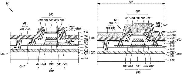
a first active layer disposed over the substrate, the first active layer including a first region, a second region spaced apart from the first region, and a first channel region disposed between the first region and the second region;
a first gate insulating film disposed on the first active layer;
a gate electrode disposed on the first gate insulating film;
a second gate insulating film disposed on the gate electrode;
a second active layer comprising at least one layer and disposed on the second gate insulating film such that the second active layer overlaps the gate electrode, the second active layer including a third region, a fourth region spaced apart from the third region, and a second channel region disposed between the third region and the fourth region;
a first electrode disposed on the third region of the second active layer; and
a second electrode spaced apart from the first electrode, disposed on the fourth region of the second active layer,
wherein an entire upper surface of the third region contacts the first electrode, and an entire upper surface of the fourth region contacts the second electrode,
wherein the second active layer includes a third auxiliary region disposed between the third region and the second channel region of the second active layer,
and a fourth auxiliary region disposed between the fourth region and the second channel region of the second active layer.
|