| CPC H01L 29/0847 (2013.01) [H01L 21/02532 (2013.01); H01L 21/02579 (2013.01); H01L 29/161 (2013.01); H01L 29/167 (2013.01); H01L 29/66636 (2013.01); H01L 29/66795 (2013.01); H01L 29/7851 (2013.01)] | 20 Claims |
|
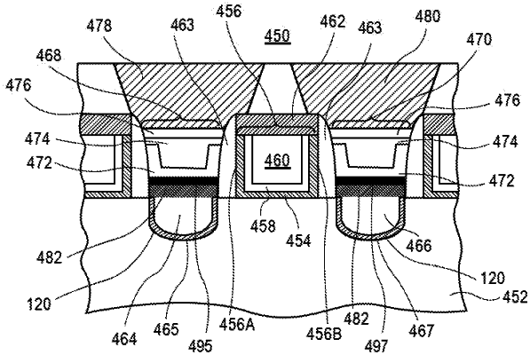
1. An integrated circuit structure, comprising:
a fin comprising silicon;
a gate structure over a channel region of the fin, the gate structure having a first side opposite a second side;
a first source or drain structure at the first side of the gate structure; and
a second source or drain structure at the second side of the gate structure, the first and second source or drain structures comprising a first semiconductor layer and a second semiconductor layer, the first semiconductor layer in contact with the channel region of the fin, and the second semiconductor layer on the first semiconductor layer, wherein the first semiconductor layer comprises a greater concentration of germanium than the second semiconductor layer, wherein the second semiconductor layer comprises boron dopant impurity atoms, and wherein the first semiconductor layer laterally surrounds the second semiconductor layer and is along a bottom of the second semiconductor layer.
|