| CPC H01L 29/0673 (2013.01) [B82Y 10/00 (2013.01); H01L 21/0262 (2013.01); H01L 21/02529 (2013.01); H01L 21/02532 (2013.01); H01L 21/02636 (2013.01); H01L 21/3081 (2013.01); H01L 21/30604 (2013.01); H01L 27/0886 (2013.01); H01L 29/0653 (2013.01); H01L 29/0692 (2013.01); H01L 29/0847 (2013.01); H01L 29/1033 (2013.01); H01L 29/401 (2013.01); H01L 29/42392 (2013.01); H01L 29/6656 (2013.01); H01L 29/66439 (2013.01); H01L 29/66545 (2013.01); H01L 29/66795 (2013.01); H01L 29/775 (2013.01); H01L 29/785 (2013.01); H01L 29/78618 (2013.01); H01L 29/78696 (2013.01); H01L 21/31053 (2013.01); H01L 21/823412 (2013.01); H01L 21/823425 (2013.01); H01L 27/088 (2013.01); H01L 29/165 (2013.01); H01L 29/1608 (2013.01)] | 16 Claims |
|
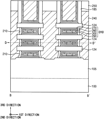
1. A method of manufacturing a semiconductor device, the method comprising:
forming a fin structure on a substrate, the fin structure comprising sacrificial lines and semiconductor lines that are alternately and repeatedly stacked;
forming a dummy gate structure on the fin structure and the substrate, the dummy gate structure comprising a dummy gate insulation pattern and a dummy gate electrode that are sequentially stacked;
etching the fin structure using the dummy gate structure as an etching mask to expose an upper surface of the substrate;
etching sidewalls of the sacrificial lines to form a first recess;
etching a portion of the dummy gate insulation pattern exposed by the first recess to form a second recess;
forming a first spacer in the first and second recesses;
forming a source/drain layer on the upper surface of the substrate; and
replacing the dummy gate structure with a gate structure.
|