| CPC H01L 27/14616 (2013.01) [G01T 1/2018 (2013.01); H01L 27/14603 (2013.01); H01L 27/14659 (2013.01); H01L 27/14663 (2013.01); H01L 27/14689 (2013.01); H01L 29/7869 (2013.01); H01L 29/78633 (2013.01); H01L 29/78666 (2013.01)] | 20 Claims |
|
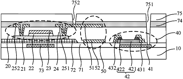
1. A drive backplane, comprising a base plate and multiple drive modules disposed on the base plate, wherein each said drive module comprises a reset transistor, a read transistor, an amplifier transistor and a memory capacitor;
the reset transistor is connected to the memory capacitor, and the reset transistor is configured to reset the memory capacitor;
the memory capacitor is connected to a photosensor, and the memory capacitor is configured to store an electric signal generated by the photosensor;
the amplifier transistor is connected to the memory capacitor, and the amplifier transistor is configured to amplify the electric signal stored in the memory capacitor;
the read transistor is connected to the amplifier transistor, and the read transistor is configured to read an electric signal amplified by the amplifier transistor;
wherein, an active layer in the amplifier transistor is made of amorphous silicon or an oxide semiconductor;
wherein the reset transistor comprises a first active layer, a first grid insulating layer, a first gate, an interlayer dielectric layer and a first source-drain electrode that are sequentially disposed on a side of the base plate;
wherein the read transistor comprises a second active layer, the first grid insulating layer, a second gate, the interlayer dielectric layer and a second source-drain electrode that are sequentially disposed on a side of the base plate;
wherein the drive backplane further comprises a buffer layer and a second grid insulating layer that are disposed between the base plate and the first active layer, and the buffer layer is disposed on a side, away from the base plate, of the second grid insulating layer;
the amplifier transistor comprises a third gate, the second grid insulating layer, a third active layer and a third source-drain electrode that are sequentially disposed on the base plate; the second source in the second source-drain electrode is connected to a third drain in the third source-drain electrode by means of a fifth via hole penetrating through the interlayer dielectric layer; and
wherein, an orthographic projection of the third active layer on the base plate does not overlap with an orthographic projection of the buffer layer on the base plate.
|