| CPC H01L 27/127 (2013.01) [H01L 27/1251 (2013.01); H01L 27/1255 (2013.01)] | 11 Claims |
|
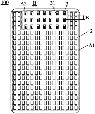
1. A display substrate having a main display area and at least one auxiliary display area located beside the main display area, comprising:
a plurality of first sub-pixels located in the main display area, and
a plurality of second sub-pixels located in each of the at least one auxiliary display area; wherein
a distribution density of the plurality of first sub-pixels in the main display area is greater than a distribution density of the plurality of second sub-pixels in each auxiliary display area;
each of the plurality of second sub-pixels includes a pixel driving circuit, and the pixel driving circuit includes at least one vertical thin film transistor and at least one capacitor; and
a space exists between every two adjacent pixel driving circuits, and a plurality of spaces constitute a light-transmitting region of a corresponding auxiliary display area,
wherein each of the at least one vertical thin film transistor includes a first electrode, a vertical active layer and a second electrode that are sequentially stacked on top of one another, and a gate arranged corresponding to the vertical active layer, and
each of the at least one capacitor includes a first electrode plate, a second electrode plate and a third electrode plate that are arranged in parallel in a direction from the first electrode to the second electrode; and the first electrode plate is electrically connected to the third electrode plate, wherein
the first electrode plate is arranged in a same layer as the gate in the pixel driving circuit to which the first electrode plate belongs; or
the first electrode plate is arranged in a same layer as the first electrode in the pixel driving circuit to which the first electrode plate belongs; and the second electrode plate is arranged in a same layer as the gate in the pixel driving circuit to which the second electrode plate belongs; or
the first electrode plate is arranged in a same layer as the second electrode in the pixel driving circuit to which the first electrode plate belongs; and the second electrode plate is arranged in a same layer as the gate in the pixel driving circuit to which the second electrode plate belongs.
|