| CPC H01L 27/1251 (2013.01) [H01L 27/1229 (2013.01); H01L 27/1255 (2013.01); H01L 27/1259 (2013.01); H01L 29/66757 (2013.01); H01L 29/66969 (2013.01)] | 20 Claims |
|
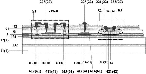
1. A display substrate, provided with a first area in which a low temperature poly-silicon transistor is deposited and a second area in which an oxide transistor is deposited, and the display substrate comprising:
a base substrate;
a first source drain layer on a side of the base substrate, wherein the first source drain layer comprises a first source electrode and a first drain electrode in the first area, and a first gate electrode in the second area;
a first active layer on a side of the first source drain layer facing away from the base substrate, wherein the first active layer comprises a poly-silicon active layer in the first area;
a first gate layer on a side of the first active layer facing away from the first source drain source drain layer, wherein the first gate layer comprises a second gate electrode and a connecting electrode in the first area, and the connecting electrode is electrically connected to the first source electrode and the first drain electrode;
a second active layer on a side of the first gate layer facing away from the first active layer, wherein the second active layer comprises an oxide active layer in the second area;
a second gate layer on a side of the second active layer facing away from the first gate layer, wherein the second gate layer comprises a third gate electrode in the second area; and
a second source drain layer on a side of the second gate layer facing away from the second active layer, wherein the second source drain layer comprises a second source electrode and a second drain electrode in the second area, and a lapping electrode in the first area, the second source electrode and the second drain electrode are electrically connected to the oxide active layer; one end of the lapping electrode is electrically connected to the connecting electrode, and another end of the lapping electrode is electrically connected to the poly-silicon active layer.
|