| CPC H01L 27/124 (2013.01) [G02F 1/13458 (2013.01); G02F 1/13629 (2021.01); H01L 27/1237 (2013.01); H01L 27/1244 (2013.01); H01L 27/1259 (2013.01)] | 16 Claims |
|
1. An array substrate, comprising:
a substrate,
three metal layers stacked on the substrate,
a plurality of signal line leads disposed in a peripheral area of the array substrate, and
a plurality of bonding pads disposed in the peripheral area, wherein
the plurality of signal line leads are distributed in at least two of the three metal layers;
the plurality of signal line leads are connected to an integrated circuit in a driving circuit through the plurality of bonding pads, and each of the plurality of bonding pads is connected to a corresponding signal line lead of the plurality of signal line leads; and
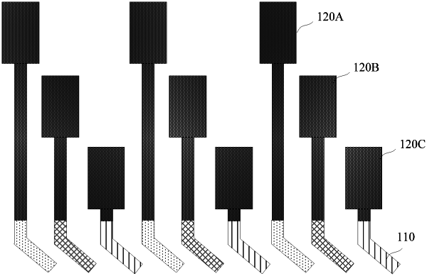
the plurality of bonding pads are disposed in a same layer and are divided into N subsets, N is equal to a number of metal layers in which the plurality of signal line leads are distributed, the plurality of bonding pads are arranged in N different lines that are parallel to each other, each subset of bonding pads are arranged in a respective line of the N different lines such that each subset of bonding pads extend to different lengths with respect to one another, and signal line leads connected to the bonding pads of each subset are distributed in a same metal layer.
|