| CPC H01L 27/1203 (2013.01) [H01L 21/823807 (2013.01); H01L 21/84 (2013.01)] | 11 Claims |
|
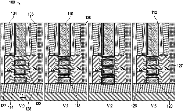
1. A semiconductor structure comprising:
a semiconductor substrate;
a first n-type field effect transistor (nFET) formed on the substrate, wherein the first nFET has a first threshold voltage (Vt0) and a gate of the first nFET comprises a gate electrode and a first work function metal (WFM) layered with a first interfacial layer (IL) and a first high-k dielectric (HK);
a second nFET formed on the substrate, wherein the second nFET has a second threshold voltage (Vt1) and a gate of the second nFET comprises a gate electrode and the first WFM layered with a second IL, a second HK, and a first dipole material; and
a third nFET formed on the substrate, wherein the third nFET has a third threshold voltage (Vt2) and a gate of the third nFET comprises a gate electrode and the first WFM layered with a third IL, a third HK, the first dipole material, and a second dipole material,
wherein the first nFET does not include the first dipole material and does not include the second dipole material, and the second nFET does not include the second dipole material, such that Vt1<Vt2<Vt0.
|