| CPC H01L 24/30 (2013.01) [H01L 23/5384 (2013.01); H01L 24/17 (2013.01); H01L 2224/1703 (2013.01)] | 16 Claims |
|
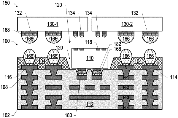
1. A method of manufacturing a microelectronic structure, the method comprising:
forming a cavity at a face of a substrate;
forming a first conductive contact of the substrate at a bottom of the cavity;
forming a second conductive contact of the substrate outside the cavity;
depositing first solder on the first conductive contact of the substrate;
depositing second solder on the second conductive contact of the substrate, wherein the first solder and the second solder have different material compositions;
placing a bridge component in the cavity, wherein the bridge component includes a first face and an opposing second face, the second face of the bridge component is between the first face of the bridge component and the substrate, the bridge component includes a first conductive contact at the first face of the bridge component, and the bridge component includes a second conductive contact at the second face of the bridge component;
coupling the second conductive contact of the bridge component to the first conductive contact of the substrate by the first solder;
placing a microelectronic component on the face of the substrate, wherein the microelectronic component has a first face and an opposing second face, the first face of the microelectronic component is between the second face of the microelectronic component and the substrate, and the microelectronic component includes conductive contacts at the first face of the microelectronic component; and
coupling a first conductive contact of the conductive contacts of the microelectronic component, by an interconnect, to the second conductive contact of the substrate, and a second conductive contact of the conductive contacts of the microelectronic component to the first conductive contact of the bridge component, wherein the interconnect includes a first layer having the first solder and a second layer having the second solder, and wherein the first layer is in contact with and in between the first conductive contact of the microelectronic component and the second layer.
|