| CPC H01L 23/5389 (2013.01) [H01L 23/00 (2013.01); H01L 24/06 (2013.01); H01L 2224/04105 (2013.01); H01L 2224/18 (2013.01); H01L 2224/24137 (2013.01); H01L 2924/18162 (2013.01)] | 5 Claims |
|
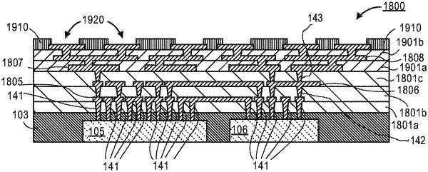
1. A device, comprising:
a first die having a first plurality of die pads;
a second die having a second plurality of die pads;
a molding layer laterally around the first die and the second die and between the first die and the second die, the molding layer laterally around the first plurality of die pads and the second plurality of die pads, wherein the molding layer has a top surface co-planar with a top surface of the first plurality of die pads and with a top surface of the second plurality of die pads;
a plurality of conductive vias directly on and in contact with the first plurality of die pads and the second plurality of die pads; and
a plurality of conductive lines directly on and in contact with the top surface of the molding layer.
|