| CPC H01L 23/5252 (2013.01) [H01L 27/0251 (2013.01); H01L 29/7833 (2013.01); H10B 20/20 (2023.02)] | 20 Claims |
|
1. An integrated circuit (IC), comprising:
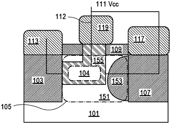
a source electrode on a source area above a substrate;
a drain electrode on a drain area above the substrate;
a channel area including a first channel region adjacent to the source area, and a second channel region adjacent to the drain area, wherein the first channel region includes a dopant of a first concentration, and the second channel region includes the dopant of a second concentration higher than the first concentration;
a gate oxide layer above the channel area;
a gate electrode above the gate oxide layer; and
a conductive path through the gate oxide layer, the conductive path coupling the source electrode and the gate electrode.
|