| CPC H01L 23/367 (2013.01) [H01L 23/22 (2013.01); H01L 23/4012 (2013.01); H01L 2023/4087 (2013.01)] | 20 Claims |
|
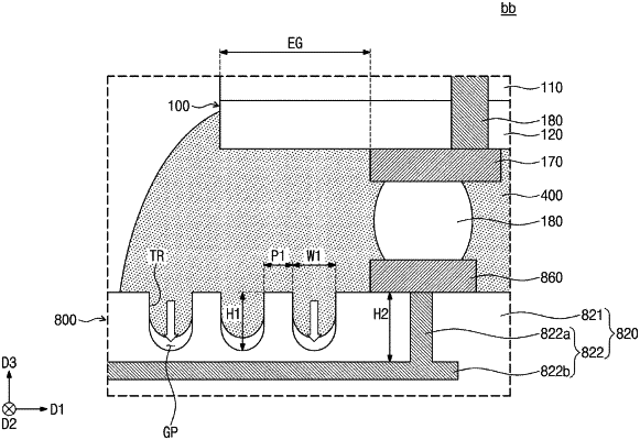
1. A semiconductor package device, comprising:
a package substrate;
an interposer on the package substrate;
a semiconductor package on the interposer; and
an under-fill between the interposer and the semiconductor package,
wherein the interposer is provided with at least one first trench at an upper portion of the interposer, the at least one first trench extending in a first direction parallel to a top surface of the package substrate,
wherein the at least one first trench vertically overlaps an edge region of the semiconductor package, and
wherein the under-fill fills at least a portion of the at least one first trench.
|