| CPC H01L 21/7684 (2013.01) [G11C 5/06 (2013.01); H01L 21/67075 (2013.01); H10B 12/09 (2023.02); H10B 63/00 (2023.02); H10N 70/801 (2023.02); H10N 70/882 (2023.02); H10N 70/883 (2023.02)] | 20 Claims |
|
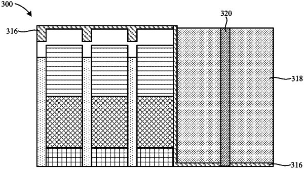
1. A method of manufacturing a memory device including a plurality of memory cells operably coupled to corresponding ones of a plurality of selectors, the method comprising:
removing a protection layer formed over the memory cells;
forming a cap layer over the memory cells;
depositing a first insulative material over the cap layer;
removing a portion of the memory cells, the selectors, the cap layer, and the first insulative material to form a socket;
depositing a second insulative material in the socket;
forming a conductive via through the second insulative material; and
etching the first insulative material to remove the first insulative material.
|