| CPC H01L 21/764 (2013.01) [H01L 21/823814 (2013.01); H01L 21/823821 (2013.01); H01L 21/823864 (2013.01); H01L 21/823878 (2013.01); H01L 27/0924 (2013.01); H01L 29/0649 (2013.01); H01L 29/6656 (2013.01); H01L 29/66795 (2013.01); H01L 29/785 (2013.01); H01L 29/7851 (2013.01); H01L 29/41791 (2013.01)] | 3 Claims |
|
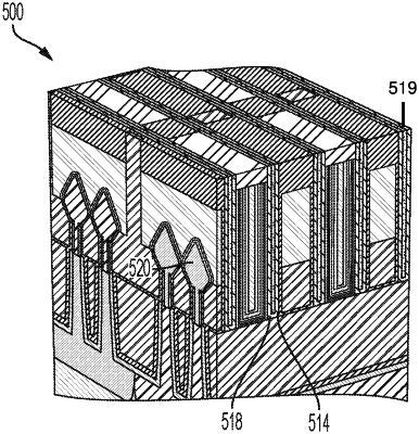
1. A semiconductor structure comprising:
a substrate;
a gate structure overlying the substrate and formed in a first direction across the substrate;
a fin overlying the substrate and formed in a second direction across the substrate, wherein the second direction is normal to the first direction, and wherein the fin intersects the gate structure;
a spacer structure adjacent the gate structure, wherein the spacer structure comprises:
a first layer adjacent the gate structure and extending a first distance laterally outward from the gate structure over the fin and the substrate; and
a second layer laterally outward from the first layer and contacting the first layer at the first distance, wherein an airgap is at least partially defined between a portion of the first layer adjacent the gate, a portion of the first layer overlying the substrate, and the second layer; and
a source/drain material formed about the fin external to the spacer structure, wherein at least one intervening layer of the spacer structure is included between the source/drain material and the airgap.
|