| CPC H01L 21/6835 (2013.01) [C30B 25/183 (2013.01); C30B 29/06 (2013.01); C30B 29/406 (2013.01); H01L 21/0242 (2013.01); H01L 21/0254 (2013.01); H01L 21/0257 (2013.01); H01L 21/02428 (2013.01); H01L 21/02458 (2013.01); H01L 21/18 (2013.01); H01L 21/28264 (2013.01); H01L 21/28587 (2013.01); H01L 21/4807 (2013.01); H01L 21/762 (2013.01); H01L 29/1033 (2013.01); H01L 29/2003 (2013.01); H01L 29/205 (2013.01); H01L 29/4175 (2013.01); H01L 29/4236 (2013.01); H01L 29/42376 (2013.01); H01L 29/66143 (2013.01); H01L 29/66204 (2013.01); H01L 29/66462 (2013.01); H01L 29/7786 (2013.01); H01L 29/7787 (2013.01); H01L 29/861 (2013.01); H01L 29/8613 (2013.01); H01L 29/872 (2013.01); H01L 29/1066 (2013.01); H01L 29/402 (2013.01); H01L 2221/6835 (2013.01); H01L 2221/68345 (2013.01)] | 20 Claims |
|
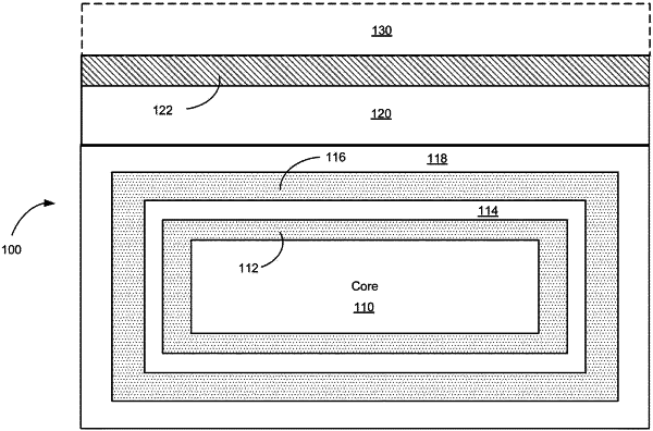
1. An integrated circuit device comprising:
a substrate comprising:
a polycrystalline ceramic core;
a first adhesion layer coupled to the polycrystalline ceramic core;
a barrier layer coupled to the first adhesion layer;
a bonding layer coupled to the barrier layer; and
a substantially single crystal layer coupled to the bonding layer;
a buffer layer coupled to the substantially single crystal layer, the buffer layer comprising a first portion and a second portion adjacent to the first portion; and
a plurality of semiconductor devices coupled to the buffer layer.
|