| CPC H01L 21/02021 (2013.01) [B24B 7/228 (2013.01); B24B 9/065 (2013.01); H01L 21/02013 (2013.01); H01L 21/67092 (2013.01); H01L 21/6838 (2013.01); H01L 21/68764 (2013.01)] | 2 Claims |
|
1. An apparatus for manufacturing a semiconductor device, comprising:
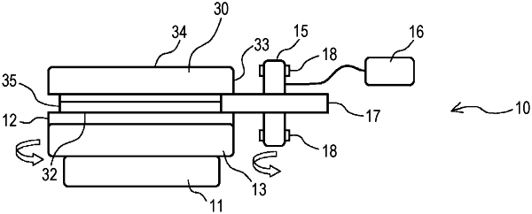
a chuck mechanism for adsorbing a semiconductor device wafer via a bonding resin layer and a support substrate with the semiconductor device surface down and rotating the semiconductor device horizontally, the support substrate being bonded to the semiconductor device surface of the semiconductor device wafer via the bonding resin layer;
a rotating blade which is rotated horizontally by a vertical spindle, to grind a circumferential edge surface of the semiconductor device wafer and an upper portion of the bonding resin layer adsorbed by the chuck mechanism and rotated horizontally; and
an ultrasonic vibration device for applying an ultrasonic wave to the vertical spindle to vibrate the rotating blade in a rotational radial direction, wherein an outer peripheral grinding wheel surface of the rotating blade is thinner than the semiconductor device wafer, the vertical spindle is journaled by bearings provided in the upper and lower portions of the vertical spindle, and the rotating blade is connected to the vertical spindle between the bearings provided in the upper portion and the lower portion of the vertical spindle.
|