| CPC H01J 37/3429 (2013.01) [B28B 1/008 (2013.01); B28B 11/24 (2013.01); C04B 35/01 (2013.01); C04B 35/453 (2013.01); C04B 35/58 (2013.01); C23C 14/086 (2013.01); C23C 14/3414 (2013.01); H01J 37/3414 (2013.01); H01J 37/3417 (2013.01); H01J 37/3426 (2013.01); H01L 21/02554 (2013.01); H01L 21/02565 (2013.01); H01L 21/02631 (2013.01); H01L 27/127 (2013.01); H01L 27/1225 (2013.01); H01L 29/42384 (2013.01); H01L 29/66969 (2013.01); H01L 29/7869 (2013.01); H01L 29/78648 (2013.01); H01L 29/78696 (2013.01); C04B 2235/3205 (2013.01); C04B 2235/3206 (2013.01); C04B 2235/3217 (2013.01); C04B 2235/3232 (2013.01); C04B 2235/3239 (2013.01); C04B 2235/3244 (2013.01); C04B 2235/3251 (2013.01); C04B 2235/3256 (2013.01); C04B 2235/3258 (2013.01); C04B 2235/3279 (2013.01); C04B 2235/3284 (2013.01); C04B 2235/3286 (2013.01); C04B 2235/3287 (2013.01); C04B 2235/3293 (2013.01); C04B 2235/3409 (2013.01); C04B 2235/3418 (2013.01); C04B 2235/3852 (2013.01); C04B 2235/72 (2013.01); C04B 2235/781 (2013.01); C04B 2235/785 (2013.01); C04B 2235/786 (2013.01); C04B 2235/80 (2013.01); G02F 1/1368 (2013.01); G02F 1/133345 (2013.01); G02F 1/133514 (2013.01); G02F 1/133553 (2013.01); G02F 2203/02 (2013.01); H01L 29/24 (2013.01)] | 8 Claims |
|
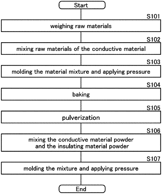
1. A method for manufacturing a sputtering target, comprising the steps of:
weighing an oxide of an element M1 and a first zinc oxide as raw materials of an insulating material;
weighing an indium oxide and a second zinc oxide as raw materials of a conductive material;
forming a first mixture by mixing the oxide of the element M1 and the first zinc oxide;
forming a first molded body by molding the first mixture with pressure;
forming a first baked body by baking the first molded body;
forming a first powder by pulverizing the first baked body;
forming a second mixture by mixing the indium oxide and the second zinc oxide;
forming a second molded body by molding the second mixture with pressure;
forming a second baked body by baking the second molded body;
forming a second powder by pulverizing the second baked body;
forming a third mixture by mixing the first powder and the second powder; and
forming a third molded body by molding the third mixture with pressure,
wherein the element M1 is one or more kinds of elements selected from Al, Ga, Si, Mg, Zr, Be and B, and
wherein baking the third molded body is not performed after forming the third molded body, or baking the third molded body is performed at a temperature at which part of the conductive material and part of the insulating material are not combined with each other after forming the third molded body.
|