US 11,735,401 B2
In-situ optical chamber surface and process sensor
Chuang-Chia Lin, San Ramon, CA (US); Upendra Ummethala, Cupertino, CA (US); Steven E. Babayan, Los Altos, CA (US); and Lei Lian, Fremont, CA (US)
Assigned to Applied Materials, Inc., Santa Clara, CA (US)
Filed by Applied Materials, Inc., Santa Clara, CA (US)
Filed on Sep. 3, 2021, as Appl. No. 17/466,912.
Application 17/466,912 is a continuation of application No. 16/378,271, filed on Apr. 8, 2019, granted, now 11,114,286.
Prior Publication US 2021/0398785 A1, Dec. 23, 2021
This patent is subject to a terminal disclaimer.
Int. Cl. G01J 3/443 (2006.01); G01J 3/02 (2006.01); H01J 37/32 (2006.01); H01J 37/22 (2006.01)
CPC H01J 37/32917 (2013.01) [G01J 3/0218 (2013.01); G01J 3/443 (2013.01); H01J 37/22 (2013.01); H01J 2237/24585 (2013.01)] 14 Claims
OG exemplary drawing
 
1. A processing tool, comprising:
a chamber; and
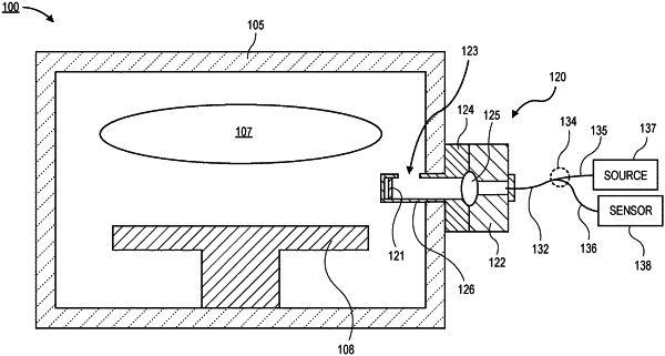
an optical sensor system that passes through a wall of the chamber, wherein the optical sensor system comprises:
a housing;
an optical path through the housing, wherein the optical path comprises a first end in the chamber and a second end outside of the chamber;
a reflector at the first end of the optic al path;
a lens between the reflector and the second end of the optical path; and
an opening through the housing between the lens and the reflector, wherein the opening is within the chamber.