US 11,735,287 B2
Buffer circuit with adaptive repair capability
Scott C. Best, Palo Alto, CA (US); John Eric Linstadt, Palo Alto, CA (US); and Paul William Roukema, Waterloo (CA)
Assigned to Rambus Inc., San Jose, CA (US)
Filed by Rambus Inc., San Jose, CA (US)
Filed on Dec. 2, 2022, as Appl. No. 18/74,188.
Application 18/074,188 is a continuation of application No. 17/368,018, filed on Jul. 6, 2021, granted, now 11,527,302.
Application 17/368,018 is a continuation of application No. 16/537,021, filed on Aug. 9, 2019, granted, now 11,069,423, issued on Jul. 20, 2021.
Application 16/537,021 is a continuation of application No. 15/506,621, granted, now 10,388,396, issued on Aug. 20, 2019, previously published as PCT/US2015/045495, filed on Aug. 17, 2015.
Claims priority of provisional application 62/041,489, filed on Aug. 25, 2014.
Prior Publication US 2023/0170039 A1, Jun. 1, 2023
Int. Cl. G11C 29/00 (2006.01); G11C 29/44 (2006.01); G11C 5/04 (2006.01); G11C 11/401 (2006.01); G11C 29/02 (2006.01); G11C 29/52 (2006.01)
CPC G11C 29/4401 (2013.01) [G11C 5/04 (2013.01); G11C 11/401 (2013.01); G11C 29/022 (2013.01); G11C 29/52 (2013.01); G11C 29/76 (2013.01); G11C 29/783 (2013.01); G11C 29/88 (2013.01); G11C 2029/4402 (2013.01)] 20 Claims
OG exemplary drawing
 
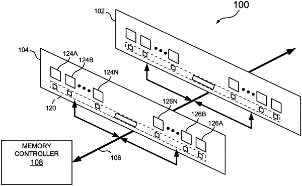
1. A command/address (C/A) buffer integrated circuit (IC) chip, comprising:
a primary C/A interface for coupling to a memory controller, the primary C/A interface to receive command and address information from the memory controller for a given data transfer operation;
a secondary C/A interface for coupling to at least one memory device;
repair circuitry to monitor the address information to detect a data transfer operation associated with known failure storage locations, the repair circuitry to generate a substitute address for a given known failure storage location associated with the data transfer operation; and
a communications interface to communicate the substitute address to at least one data buffer IC chip.