| CPC G09G 3/3258 (2013.01) [G09G 3/3266 (2013.01); G09G 3/3291 (2013.01); G09G 2310/0278 (2013.01); G09G 2310/061 (2013.01)] | 20 Claims |
|
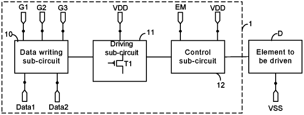
1. A pixel driving circuit, comprising a data writing sub-circuit, a driving sub-circuit, and a control sub-circuit; the driving sub-circuit including a driving transistor, wherein
the data writing sub-circuit is connected to a first scanning signal terminal, a second scanning signal terminal, a third scanning signal terminal, a first data signal terminal, a second data signal terminal, and the driving sub-circuit; and the data writing sub-circuit is configured to: in response to a first scanning signal received from the first scanning signal terminal and a third scanning signal received from the third scanning signal terminal, write a first data signal provided from the first data signal terminal into the driving sub-circuit, to and compensate for a threshold voltage of the driving transistor; and in response to a second scanning signal received from the second scanning signal terminal and the third scanning signal received from the third scanning signal terminal, write a second data signal provided from the second data signal terminal into the driving sub-circuit, and compensate for the threshold voltage of the driving transistor;
the control sub-circuit is connected to an enable signal terminal, a first power supply voltage signal terminal, the driving sub-circuit; the control sub-circuit is configured to be connected to an element to be driven; and the control sub-circuit is configured to, in response to an enable signal received from the enable signal terminal, connect the first power supply voltage signal terminal to the driving transistor, and connect the driving transistor to the element to be driven;
the driving sub-circuit is further connected to the first power supply voltage signal terminal; and the driving sub-circuit is configured to: according to the first data signal and a first power supply voltage signal provided from the first power supply voltage signal terminal, output a driving signal to the element to be driven, so as to drive the element to be driven to operate; and according to the second data signal and the first power supply voltage signal, control the element to be driven to be in an operating state or in a non-operating state;
the driving transistor is configured to be turned on and in a saturation state according to the second data signal, or be turned off according to the second data signal.
|