| CPC G09G 3/3258 (2013.01) [G09G 3/3233 (2013.01); G09G 2300/0426 (2013.01); G09G 2300/0819 (2013.01); G09G 2300/0852 (2013.01); G09G 2310/0251 (2013.01); G09G 2310/061 (2013.01); G09G 2320/0233 (2013.01); G09G 2320/0247 (2013.01); G09G 2320/043 (2013.01)] | 15 Claims |
|
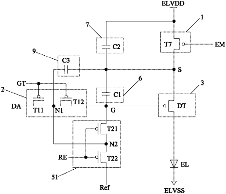
1. A pixel driving circuit for driving a light-emitting element, comprising:
a driving transistor, wherein a second electrode of the driving transistor is connected to the light-emitting element;
a power control sub-circuit, respectively connected to a first control terminal, a power signal input terminal and a first electrode of the driving transistor;
a data writing-in sub-circuit, respectively connected to a first common node, a gate line of a corresponding row, a data line of a corresponding column and a gate electrode of the driving transistor, and configured to, under the control of the gate line, control to connect or disconnect the data line and the first common node, and control to connect or disconnect the first common node and the gate electrode of the driving transistor;
a first reset control sub-circuit, respectively connected to a second common node, a reset signal line, the gate electrode of the driving transistor and a reference voltage input terminal; configured to, under the control of the reset signal line, control to connect or disconnect the reference voltage input terminal and the second common node, and control to connect or disconnect the second common node and the gate electrode of the driving transistor;
a first capacitor unit, wherein a first end of the first capacitor unit is connected to the gate electrode of the drive transistor, and a second end of the first capacitor unit is connected to the first electrode of the drive transistor;
a second capacitor unit, wherein a first end of the second capacitor unit is connected to the first electrode of the driving transistor, and a second end of the second capacitor unit is connected to the power signal input terminal; and
a third capacitor unit, a first end of the third capacitor unit is connected to the first common node and/or the second common node, and a second end of the third capacitor unit is connected to the first electrode of the driving transistor.
|