| CPC G09G 3/3225 (2013.01) [G11C 19/28 (2013.01); H10K 59/124 (2023.02); H10K 59/1213 (2023.02); H10K 59/131 (2023.02); H10K 71/00 (2023.02); G09G 2300/0426 (2013.01); G09G 2310/0286 (2013.01); H10K 59/1201 (2023.02)] | 20 Claims |
|
1. A display substrate, comprising: a base substrate, and a shift register unit, a first clock signal line, a second clock signal line that are on the base substrate,
wherein the first clock signal line extends along a first direction on the base substrate and is configured to provide a first clock signal to the shift register unit;
the second clock signal line extends along the first direction on the base substrate and is configured to provide a second clock signal to the shift register unit;
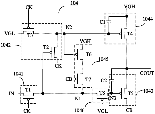
the shift register unit comprises an input circuit, an output circuit, a first control circuit, a second control circuit, and an output control circuit;
the input circuit is configured to input an input signal to a first node in response to the first clock signal;
the output circuit is configured to output an output signal to an output terminal;
the first control circuit is configured to control a level of a second node in response to a level of the first node and the first clock signal;
the second control circuit is connected to the first node and the second node and is configured to control the level of the first node under control of the level of the second node and the second clock signal; and
the output control circuit is configured to control a level of the output terminal under control of the level of the second node,
wherein the first control circuit comprises a first control transistor and a second control transistor, the second control circuit comprises a first noise reduction transistor and a second noise reduction transistor, and the shift register unit further comprises an intermediate transfer electrode;
an active layer of the first control transistor and an active layer of the second control transistor are arranged side by side with an active layer of the first noise reduction transistor and an active layer of the second noise reduction transistor in a second direction different from the first direction;
an orthographic projection of the intermediate transfer electrode on the base substrate is between a whole of an orthographic projection of the active layer of the first control transistor on the base substrate and an orthographic projection of the active layer of the second control transistor on the base substrate and a whole of an orthographic projection of the active layer of the first noise reduction transistor on the base substrate and an orthographic projection of the active layer of the second noise reduction transistor on the base substrate; and
a gate electrode of the first noise reduction transistor is connected to a first electrode of the first control transistor and a first electrode of the second control transistor through the intermediate transfer electrode.
|