| CPC G09G 3/32 (2013.01) [G09G 2300/0408 (2013.01); G09G 2310/0286 (2013.01); G09G 2310/0297 (2013.01); G09G 2310/08 (2013.01); G09G 2320/0223 (2013.01); G09G 2330/026 (2013.01)] | 17 Claims |
|
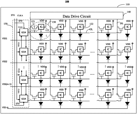
1. An electronic substrate, comprising a pixel drive chip which comprises at least one signal terminal, a signal generation circuit, a data storage circuit, and an output circuit,
wherein the at least one signal terminal is configured to be electrically connected to a light-emitting element;
the signal generation circuit is connected to the at least one signal terminal, and is configured to receive an input signal through the at least one signal terminal and generate a clock signal according to the input signal;
the data storage circuit is connected to the signal generation circuit and the output circuit, and is configured to receive the clock signal and store the input signal according to the clock signal; and
the output circuit is configured to output a current, which is generated according to the input signal stored and used for driving the light-emitting element, through the at least one signal terminal,
wherein the signal generation circuit is further configured to generate a data delay signal according to the input signal, generate a data enable signal according to a difference between the data delay signal and the input signal, and generate the clock signal according to the data enable signal,
wherein the data storage circuit comprises a latch and a shift register;
the latch is connected to the signal generation circuit and is configured to store the input signal and the data enable signal; and
the shift register is connected to the latch and the output circuit, and is configured to shift and store the input signal according to the clock signal,
wherein a level of the input signal, a level of the data enable signal, and a level of the clock signal are higher than a bias voltage of a data signal and a bias voltage of a first power supply voltage.
|