| CPC G09G 3/2003 (2013.01) [G09G 2310/027 (2013.01); G09G 2310/0297 (2013.01); G09G 2330/021 (2013.01)] | 12 Claims |
|
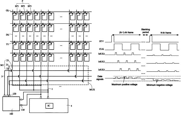
1. A method of driving a display panel, wherein the display panel comprises a multiplexing unit and a plurality of pixels arranged in an array of M rows and N columns, the multiplexing unit comprises a plurality of thin film transistors, and each thin film transistor of the multiplexing unit comprises a gate electrode applied with a multiplexing unit gate signal, a first electrode applied with a data signal, and a second electrode electrically connected to a pixel driving circuit of a pixel; and wherein the method comprises:
acquiring a plurality of data signals for driving i-th row of pixels, where 1≤i≤M;
generating multiplexing unit gate signals for respective thin film transistors of the multiplexing unit based on the plurality of data signals; and
applying the multiplexing unit gate signals to gate electrodes of the respective thin film transistors, so that the respective thin film transistors of the multiplexing unit are turned on or turned off,
wherein the multiplexing unit gate signals change according to changes of the plurality of data signals; and
wherein the plurality of data signals for driving the i-th row of pixels comprise a plurality of positive voltage signals and a plurality of negative voltage signals, and the method further comprises:
determining a maximum positive voltage which has a maximum value among the plurality of positive voltage signals; and
determining a minimum negative voltage which has a minimum absolute value among the plurality of negative voltage signals.
|