| CPC G09G 3/20 (2013.01) [G11C 19/28 (2013.01); G09G 2310/0267 (2013.01); G09G 2310/0286 (2013.01); G09G 2310/061 (2013.01)] | 16 Claims |
|
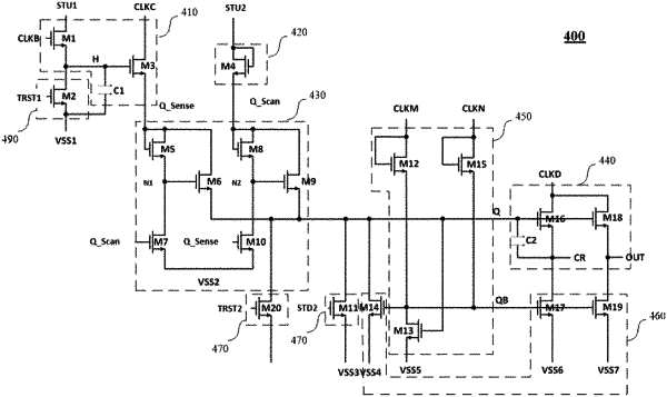
1. A shift register, comprising:
a first input sub-circuit, configured to receive a first input signal from a first input terminal and output a blanking output control signal;
a second input sub-circuit, configured to receive a second input signal from a second input terminal and output a display output control signal, wherein the second input signal is a turn-on signal of a high level; and
an output sub-circuit, configured to output a composite output signal via an output terminal under control of a first node, the composite output signal including a display output signal outputted in a display period of time and a blanking output signal outputted in a blanking period of time which are independent of each other,
wherein the second input sub-circuit comprises a first display input transistor and a second display input transistor, and an electrode of the first display input transistor is connected to an electrode of the second display input transistor,
wherein a first electrode of the first display input transistor is connected to a high level signal line, a control electrode of the first display input transistor is connected to a display input signal line or an output terminal of another shift register, and a second electrode of the first display input transistor is connected to an electrode of the second display input transistor.
|