| CPC G09G 3/20 (2013.01) [G09G 2310/0275 (2013.01); G09G 2330/028 (2013.01)] | 21 Claims |
|
1. A display device comprising:
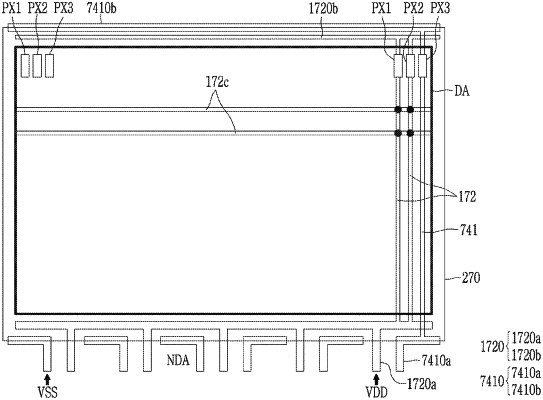
a substrate including a display area and a non-display area;
an external common voltage line, an external initialization voltage line, and an external driving voltage line disposed in the non-display area;
a plurality of pixels and a common voltage line disposed in the display area; and
a driving voltage line connected to each of the plurality of pixels,
wherein a subset of the plurality of pixels overlaps the common voltage line in the display area in a plan view,
the external common voltage line and the common voltage line are connected to each other, and
each of the external initialization voltage line, the external driving voltage line, and the external common voltage line includes a plurality of portions that are separated from each other.
|