| CPC G02F 1/1368 (2013.01) [G02F 1/134318 (2021.01); G02F 1/136227 (2013.01); G02F 1/136286 (2013.01)] | 16 Claims |

|
1. An array substrate, comprising:
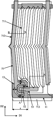
a plurality of sub-pixel units arranged in an array, each sub-pixel unit of the plurality of sub-pixel units comprising a base substrate, a thin film transistor, a pixel electrode and a common electrode, the common electrode being on a side of the base substrate, the thin film transistor and the pixel electrode being between the base substrate and the common electrode, the thin film transistor comprising a control terminal, a first electrode and a second electrode, the pixel electrode being connected to the second electrode, and the control terminal being in a continuous sheet shape, an orthographic projection of a boundary of the control terminal on the base substrate being within an orthographic projection of the common electrode on the base substrate,
wherein a portion of the common electrode corresponding to the control terminal comprises an opening, an orthographic projection of the control terminal on the base substrate and the orthographic projection of the common electrode on the base substrate have a first overlap area, and the first overlap area surrounds an orthographic projection of the opening on the base substrate.
|