US 11,733,507 B2
Optical device, method of using the same, and method of making the same
Piotr Nyga, West Lafayette, IN (US); Alexander V. Kildishev, West Lafayette, IN (US); Sarah Nahar Chowdhury, West Lafayette, IN (US); Alexandra Boltasseva, West Lafayette, IN (US); Zhaxylyk Kudyshev, West Lafayette, IN (US); and Vladimir M. Shalaev, West Lafayette, IN (US)
Assigned to Purdue Research Foundation, West Lafayette, IN (US)
Filed by Purdue Research Foundation, West Lafayette, IN (US)
Filed on Feb. 19, 2020, as Appl. No. 16/794,964.
Claims priority of provisional application 62/807,606, filed on Feb. 19, 2019.
Prior Publication US 2020/0285043 A1, Sep. 10, 2020
Int. Cl. G02F 1/01 (2006.01); G02B 26/00 (2006.01)
CPC G02B 26/007 (2013.01) [G02F 1/0147 (2013.01); G02B 2207/101 (2013.01); G02F 2203/10 (2013.01)] 20 Claims
OG exemplary drawing
 
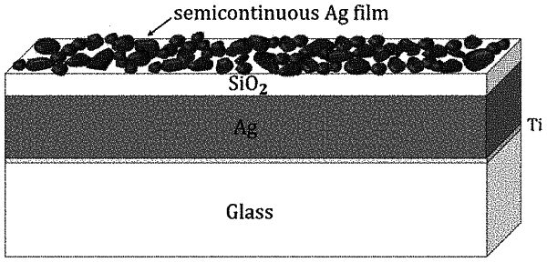
1. An optical device comprising:
a substrate;
a wetting layer;
a dielectric layer over a mirror layer;
a plurality of plasmonic nanoparticles over the dielectric layer; and
a protective layer over the plurality of plasmonic nanoparticles,
wherein the mirror layer and the wetting layer are over the substrate.