US 11,733,077 B2
Carrier for measurement and wafer transfer system including the same
Sanga Bang, Hwaseong-si (KR); Geunhyung Kim, Hwaseong-si (KR); Sangmin Kim, Hwaseong-si (KR); Gi-Nam Park, Incheon (KR); Chul-Jun Park, Seoul (KR); Yong-Jun Ahn, Suwon-si (KR); JongJin Ahn, Hwaseong-si (KR); Min Kyun Lee, Suwon-si (KR); Sangkyung Lee, Hwaseong-si (KR); and Kyubum Cho, Hwaseong-si (KR)
Assigned to SAMSUNG ELECTRONICS CO., LTD.
Filed by SAMSUNG ELECTRONICS CO., LTD., Suwon-si (KR)
Filed on Oct. 18, 2021, as Appl. No. 17/504,212.
Claims priority of application No. 10-2021-0040655 (KR), filed on Mar. 29, 2021.
Prior Publication US 2022/0307877 A1, Sep. 29, 2022
Int. Cl. G01F 1/42 (2006.01); G01F 1/37 (2006.01)
CPC G01F 1/42 (2013.01) [G01F 1/37 (2013.01)] 20 Claims
OG exemplary drawing
 
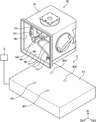
1. A measurement carrier, comprising:
a housing having an internal space; and
a flow-rate measuring device located within the internal space,
wherein a bottom surface of the housing comprises a first inflow hole, a second inflow hole, and an outflow hole, each of which is configured to provide fluid communication between the internal space and an outer space,
wherein the flow-rate measuring device comprises:
a first flow-rate measuring sensor in fluid communication with the first inflow hole; and
a second flow-rate measuring sensor in fluid communication with the second inflow hole.