| CPC C23C 16/45542 (2013.01) [C23C 16/0209 (2013.01); C23C 16/45546 (2013.01); C23C 16/45553 (2013.01); H01L 21/56 (2013.01); H10N 70/023 (2023.02)] | 18 Claims |
|
1. A method of forming an encapsulation stack, the method comprising:
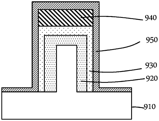
providing a substrate with a surface having at least one feature thereon, the surface comprising a film stack with a first exposed material and a second exposed material, the first exposed material comprising carbon and the second exposed material comprising a chalcogen, the feature having a height and width defining an aspect ratio;
forming a conformal dielectric protective layer directly on the first exposed material and the second exposed material by sequentially exposing the substrate to a first reactant and a second reactant, the protective layer comprising silicon nitride, and the first reactant comprising SiRaXb, where R is an organic group or H, X is a halogen, and a+b=4; and
forming a conformal hermetic encapsulation layer on the protective layer by sequentially exposing the substrate to a silicon precursor and a nitrogen precursor and a second plasma, the encapsulation layer comprising silicon nitride, wherein the substrate is maintained at a temperature less than or equal to about 250° C.,
wherein the protective layer is formed at a rate of greater than or equal to about 1 Å/min and the protective layer is formed without damaging the second exposed material.
|