| CPC C23C 14/35 (2013.01) [H01J 37/3405 (2013.01); H01J 37/3488 (2013.01)] | 18 Claims |
|
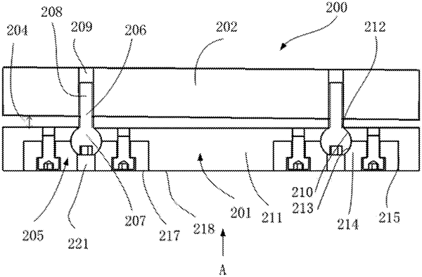
1. A physical vapor deposition (PVD) chamber, comprising a chamber body, and an upper electrode assembly being arranged in the chamber body and including:
a base plate assembly configured to carry a magnetron;
a backplate arranged at an interval with the base plate assembly; and
a connection assembly for connecting the base plate assembly to the backplate, the backplate being arranged on a side of the base plate assembly away from the magnetron;
wherein:
the connection assembly includes a connection bolt;
a bolt head of the connection bolt is connected to the base plate assembly;
a bolt is threadedly connected to the backplate, and
the bolt head is located inside the base plate assembly, an operation hole is arranged on a side of the base plate assembly away from the backplate to expose the bolt head, and an operation slot is arranged at the bolt head corresponding to the operation hole.
|