US 11,732,297 B2
Methods and apparatus for measuring analytes using large scale FET arrays
Jonathan Rothberg, Guilford, CT (US); Wolfgang Hinz, Killingworth, CT (US); Kim Johnson, Carlsbad, CA (US); and James Bustillo, Castro Valley, CA (US)
Assigned to Life Technologies Corporation, Carlsbad, CA (US)
Filed by Life Technologies Corporation, Carlsbad, CA (US)
Filed on May 6, 2022, as Appl. No. 17/738,427.
Application 15/216,242 is a division of application No. 14/703,565, filed on May 4, 2015, abandoned.
Application 17/738,427 is a continuation of application No. 16/846,113, filed on Apr. 10, 2020, granted, now 11,339,430.
Application 16/846,113 is a continuation of application No. 15/949,456, filed on Apr. 10, 2018, granted, now 10,633,699, issued on Apr. 28, 2020.
Application 15/949,456 is a continuation of application No. 15/216,242, filed on Jul. 21, 2016, granted, now 9,951,382, issued on Apr. 24, 2018.
Application 14/703,565 is a continuation of application No. 13/866,582, filed on Apr. 19, 2013, granted, now 9,023,189, issued on May 5, 2015.
Application 13/866,582 is a continuation of application No. 13/616,454, filed on Sep. 14, 2012, granted, now 8,535,513, issued on Sep. 17, 2013.
Application 13/616,454 is a continuation of application No. 13/149,262, filed on May 31, 2011, granted, now 8,317,999, issued on Nov. 27, 2012.
Application 13/149,262 is a continuation of application No. 12/002,781, filed on Dec. 17, 2007, granted, now 8,262,900, issued on Sep. 11, 2012.
Application 12/002,781 is a continuation in part of application No. 12/002,291, filed on Dec. 14, 2007, granted, now 7,948,015, issued on May 24, 2011.
Claims priority of provisional application 60/956,324, filed on Aug. 16, 2007.
Claims priority of provisional application 60/948,748, filed on Jul. 10, 2007.
Claims priority of provisional application 60/870,073, filed on Dec. 14, 2006.
Prior Publication US 2022/0340965 A1, Oct. 27, 2022
Int. Cl. C12Q 1/6869 (2018.01); H01L 23/00 (2006.01); H01L 29/78 (2006.01); G01N 27/414 (2006.01); C12Q 1/6874 (2018.01); H01L 21/306 (2006.01); H01L 27/088 (2006.01)
CPC C12Q 1/6869 (2013.01) [C12Q 1/6874 (2013.01); G01N 27/414 (2013.01); G01N 27/4145 (2013.01); G01N 27/4148 (2013.01); H01L 21/306 (2013.01); H01L 24/18 (2013.01); H01L 24/20 (2013.01); H01L 24/82 (2013.01); H01L 27/088 (2013.01); H01L 29/78 (2013.01); H01L 2224/04105 (2013.01); H01L 2924/1306 (2013.01); H01L 2924/13091 (2013.01); H01L 2924/1433 (2013.01)] 20 Claims
OG exemplary drawing
 
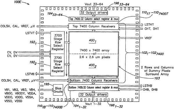
1. A semiconductor device comprising:
a sensor array arranged in a plurality of rows and a plurality of columns, and a microwell array formed over the sensor array, wherein the sensor array comprises a first group of sensors and a second group of sensors; and
sensor array circuitry on the semiconductor device for separate control of the first group of sensors and the second group of sensors; said sensor array circuitry including:
a first row select register to apply a sequence of row select signals to enable the first group of sensors and a second row select register to apply a sequence of row select signals to enable the second group of sensors;
a first column select register to acquire output signals from respective columns of the first group of sensors and a second column select-register to acquire output signals from respective columns of the second group of sensors; and
a first column bias/readout circuit for receiving column output signals from the first group of sensors and a second column bias/readout circuit for receiving column output signals from the second group of sensors.