| CPC B24B 37/005 (2013.01) [B24B 37/26 (2013.01); B24B 41/06 (2013.01); H01L 21/30625 (2013.01)] | 23 Claims |
|
1. A system, comprising:
a rotatable head for mounting a wafer thereto;
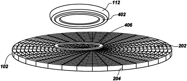
a polishing pad mounted to a rotatable platen, the polishing pad comprising an array of piezoelectric actuators, each piezoelectric actuator of the array of piezoelectric actuators configured to convert applied electrical energy to mechanical stress resulting in dimensional displacement of a thickness thereof in a direction orthogonal to a direction of rotation of the polishing pad to modify a surface of the polishing pad and configured to convert applied mechanical stress to output electrical energy;
a fluid dispenser for dispensing a fluid onto the polishing pad; and
a controller operably couple to the array of piezoelectric actuators, the controller comprising:
at least one processor; and
at least one non-transitory computer-readable storage medium storing instructions thereon that, when executed by the at least one processor, cause the controller to determine a topography of at least a portion of a surface of the wafer based on voltages output by the piezoelectric actuators of the array of piezoelectric actuators, determine a counter surface topography for at least a portion of the polishing pad based on the topography of the at least the portion of the surface of the wafer, and apply electrical energy to one or more piezoelectric actuators of the array of piezoelectric actuators to modify the polishing pad to include the counter surface topography.
|