| CPC H10N 70/066 (2023.02) [H10B 63/20 (2023.02); H10B 63/22 (2023.02); H10B 63/82 (2023.02); H10B 63/84 (2023.02)] | 16 Claims |
|
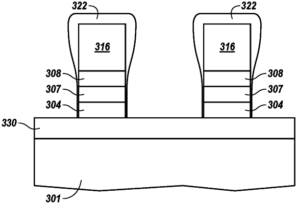
1. A memory cell, comprising:
a plurality of stack structures in a length direction parallel to one another, and separated from each other in a first direction perpendicular to the length direction, wherein each of the plurality of stack structures comprises;
plural select device stacks; and
a dielectric material comprising plural segments;
an electrode material formed in plural segments, each electrode segment extending in the length direction; and
a non-conformal encapsulating material encapsulating the electrode material, such that there is encapsulating material on an entire top surface of the memory cell and on side surfaces of the memory cell,
wherein the top surface comprises a programmable material, and the side surfaces comprise the first electrode, the second electrode, and the select device, and
wherein more of the encapsulating material is on a top surface of the memory cell than on the side surfaces of the memory cell.
|