| CPC H01L 27/18 (2013.01) [G02B 6/29341 (2013.01); G06N 10/00 (2019.01); H01L 39/025 (2013.01); H01L 39/223 (2013.01)] | 20 Claims |
|
1. A method for quantum computing, the method comprising:
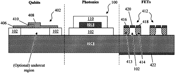
providing a computing device that includes: (i) a waveguide structure comprising a wafer, and a waveguide disposed on the wafer, the waveguide comprising a resonator-based microwave-to-optical transducer having a silicon germanium (SiGe) core surrounded by silicon (Si), wherein the wafer has a lower refractive index than the Si, (ii) quantum bits (qubits) disposed on the wafer, (iii) superconducting bus paths between the waveguide and the qubits, and (iv) field effect transistors (FETs) disposed on the wafer connecting the superconducting bus paths between the waveguide and the qubits;
selecting one of the superconducting bus paths between the waveguide and a given one of the qubits;
routing a microwave signal from the given one of the qubits along the one of the superconducting bus paths that has been selected; and
converting the microwave signal to an optical signal via the resonator-based microwave-to-optical transducer.
|