| CPC H10N 52/80 (2023.02) [G11C 11/161 (2013.01); G11C 11/1673 (2013.01); G11C 11/1675 (2013.01); G11C 11/18 (2013.01); H10B 61/22 (2023.02); H10N 52/00 (2023.02); H10N 52/01 (2023.02)] | 15 Claims |
|
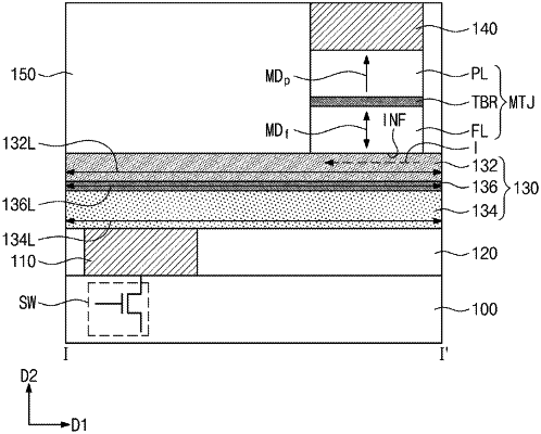
1. A magnetic memory device, comprising:
a lower electrode on a substrate;
a conductive line on the lower electrode; and
a magnetic tunnel junction pattern on the conductive line,
wherein:
the conductive line includes:
a first conductive line adjacent to the magnetic tunnel junction pattern;
a second conductive line between the lower electrode and the first conductive line; and
a high resistance layer at least partially between the first conductive line and the second conductive line,
a resistivity of the second conductive line is lower than a resistivity of the first conductive line,
a resistivity of the high resistance layer is higher than the resistivity of the first conductive line and higher than the resistivity of the second conductive line,
at least a portion of the high resistance layer is vertically overlapped with the magnetic tunnel junction pattern,
each of the first conductive line, the second conductive line, and the high resistance layer has a thickness in a direction perpendicular to a top surface of the substrate, and
the thickness of the high resistance layer is smaller than the thickness of the first conductive line and smaller than the thickness of the second conductive line.
|