| CPC H10N 50/80 (2023.02) [G11C 11/161 (2013.01); H10N 50/85 (2023.02)] | 17 Claims |
|
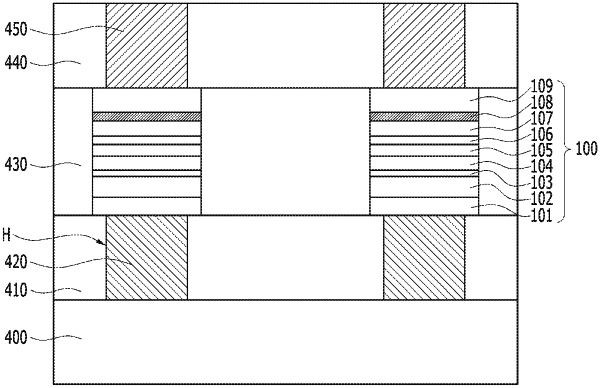
1. An electronic device comprising a semiconductor memory, wherein the semiconductor memory includes:
a magnetic tunnel junction (MTJ) structure including a free layer, a pinned layer, and a tunnel barrier layer, the free layer having a variable magnetization direction, the pinned layer having a fixed magnetization direction, the tunnel barrier layer being interposed between the free layer and the pinned layer; and
a thermal stability enhanced layer (TSEL) including a homogeneous material having an Fe—O bond,
wherein the semiconductor memory includes a synthetic antiferromagnet (SAF) structure disposed over the tunnel barrier layer and the TSEL is disposed under the free layer.
|