| CPC H10N 30/10513 (2023.02) [H10N 30/04 (2023.02); H10N 30/067 (2023.02); H10N 30/877 (2023.02); H10N 30/063 (2023.02)] | 20 Claims |
|
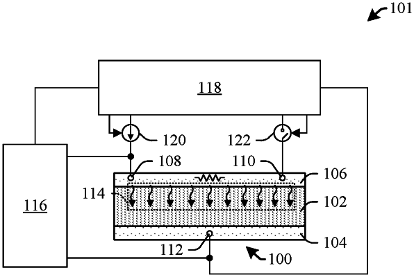
16. A piezoelectric device, comprising:
a semiconductor substrate;
a piezoelectric structure disposed over the semiconductor substrate and vertically between a first electrode and a second electrode;
a heating structure disposed over the semiconductor substrate, wherein the heating structure is spaced from each of the first electrode, the piezoelectric structure, and the second electrode, and wherein the heating structure is configured to heat the piezoelectric structure to a recovery temperature for a period of time;
a first passivation layer disposed over the first electrode, the piezoelectric structure, and the second electrode, wherein the first passivation layer extends along sidewalls of the first electrode, the piezoelectric structure, and the second electrode;
a first conductive pad disposed over the semiconductor substrate and electrically coupled to the first electrode, wherein the first conductive pad extends vertically through the first passivation layer to contact the first electrode at a first location;
a second conductive pad disposed over the semiconductor substrate and electrically coupled to the second electrode, wherein the second conductive pad extends vertically through the first passivation layer to contact the second electrode at a second location that is spaced from the first location;
a third conductive pad disposed over the semiconductor substrate and electrically coupled to the heating structure, wherein the third conductive pad contacts the heating structure at a third location, and wherein the third location is spaced from both the first location and the second location; and
a fourth conductive pad disposed over the semiconductor substrate and electrically coupled to the heating structure, wherein the fourth conductive pad contacts the heating structure at a fourth location, and wherein the fourth location is spaced from each of the first location, the second location, and the third location.
|