| CPC H10K 59/40 (2023.02) [H10K 50/844 (2023.02); H10K 50/865 (2023.02); H10K 59/121 (2023.02)] | 13 Claims |
|
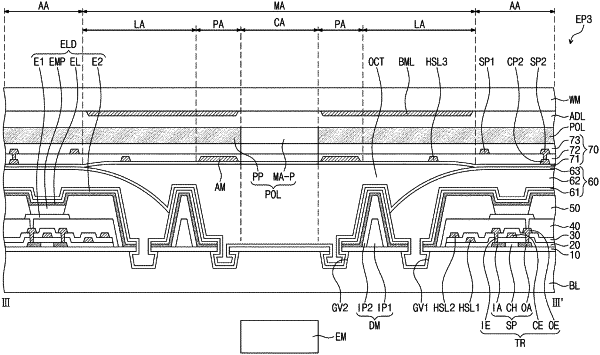
1. A display device comprising:
an electronic module; and
an electronic panel including:
a base layer including an upper surface having a recessed portion and a dam portion; and
an alignment mark including a conductive pattern disposed on the base layer, wherein the electronic panel includes:
a first area including the electronic module;
a second area surrounding at least a portion of the first area in a plan view;
a light blocking layer disposed in the second area, and
an active area surrounding at least a portion of the second area in a plan view, wherein:
the recessed portion and the dam portion are disposed in the second area,
the second area includes a pattern area surrounding the first area and a line area surrounding the pattern area,
the alignment mark is disposed between the base layer and the light blocking layer, and disposed in the pattern area.
|