| CPC H10K 59/1315 (2023.02) [H10K 59/126 (2023.02); H10K 59/38 (2023.02); H10K 71/00 (2023.02); H10K 59/1201 (2023.02)] | 18 Claims |
|
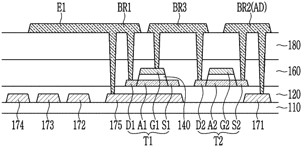
1. A display device comprising:
a substrate;
a data line on the substrate;
a first insulating layer on the data line;
a first transistor on the first insulating layer;
a second transistor on the first insulating layer;
a second insulating layer on the first transistor;
a pixel electrode on the second insulating layer, the pixel electrode being electrically connected to the first transistor;
an auxiliary data pattern on the second insulating layer as a same layer as the pixel electrode, the auxiliary data pattern being electrically connected to the data line;
a light blocking layer between the substrate and the first insulating layer, the light blocking layer overlapping a channel region of the first transistor; and
a first bridge on the second insulating layer as a same layer as the pixel electrode, the first bridge being connected to the pixel electrode, an electrode of the first transistor, and the light blocking layer,
wherein the display device further comprises a data driver to apply a data voltage to the data line, and the data line is to transmit the data voltage to the second transistor.
|