| CPC H10K 59/131 (2023.02) [H10K 59/126 (2023.02); H10K 59/1213 (2023.02); H10K 59/1216 (2023.02); H10K 59/65 (2023.02)] | 19 Claims |
|
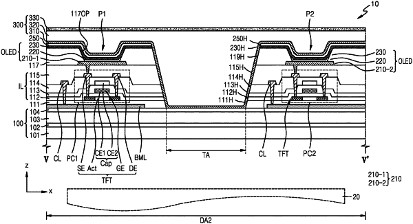
1. A display device having a display area and a peripheral area adjacent to the display area, the display device comprising:
a substrate;
a plurality of pixel circuits in the display area, the pixel circuits each comprising a thin film transistor and a capacitor, the thin film transistor including a semiconductor layer and a gate electrode on the substrate and the capacitor including a first capacitor plate and a second capacitor plate;
a plurality of signal lines electrically connected to the pixel circuits, the signal lines passing through the display area;
a lower metal layer between the substrate and at least one of the pixel circuits;
a pad portion in the peripheral area; and
a plurality of wirings in the peripheral area, the plurality of wirings electrically connecting the pad portion to the signal lines,
wherein the plurality of wirings further comprise:
a first wiring at a same layer as the lower metal layer; and
a second wiring above the first wiring with a first insulating layer between the first wiring and the second wiring,
wherein a first portion of the first insulating layer is between the first wiring and the second wiring, and a second portion of the first insulating layer is between the substrate and the pixel circuits.
|