| CPC H10K 59/131 (2023.02) [H10K 59/123 (2023.02); H10K 59/124 (2023.02); H10K 59/60 (2023.02); H10K 19/20 (2023.02); H10K 59/121 (2023.02)] | 11 Claims |
|
1. A display apparatus comprising:
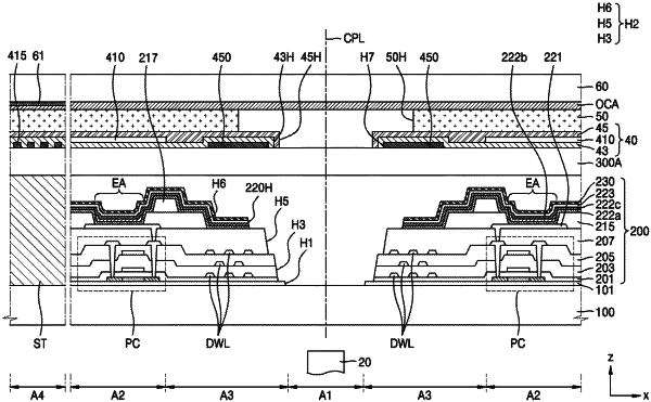
a substrate;
a buffer layer on the substrate;
a first hole penetrating the buffer layer and exposing an upper surface of the substrate;
a display layer on the buffer layer, the display layer comprising display elements and bypass lines;
a second hole penetrating the display layer and connected to the first hole,
wherein the bypass lines extend along a portion of a perimeter of the second hole and are disposed between the second hole and the display elements;
a component overlapping the first hole and disposed directly below the substrate; and
an encapsulation member covering the display elements and the bypass lines,
wherein at least a portion of an upper surface of the buffer layer is exposed by the second hole.
|