| CPC H10K 59/122 (2023.02) [H10K 71/00 (2023.02); H10K 2102/103 (2023.02)] | 6 Claims |
|
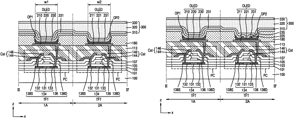
1. A method of manufacturing a display device, the method including:
preparing a substrate including a display area, the display area including a first area and a second area;
forming a first pixel electrode in the first area, and a second pixel electrode in the second area;
forming a pixel-defining layer including a first opening and a second opening, the first opening being in the first pixel electrode and exposing at least a portion of the first pixel electrode, and the second opening being in the second pixel electrode and exposing at least a portion of the second pixel electrode;
forming a first intermediate layer on the at least a portion of the first pixel electrode, and a second intermediate layer on the at least a portion of the second pixel electrode;
forming a hydrophobic layer on the second intermediate layer;
forming a first opposite electrode on the first intermediate layer and the hydrophobic layer;
removing the hydrophobic layer and the first opposite electrode on the hydrophobic layer; and
forming a second opposite electrode on the first opposite electrode and the second intermediate layer.
|