| CPC H10K 59/122 (2023.02) [H10K 59/131 (2023.02); H10K 59/88 (2023.02)] | 20 Claims |
|
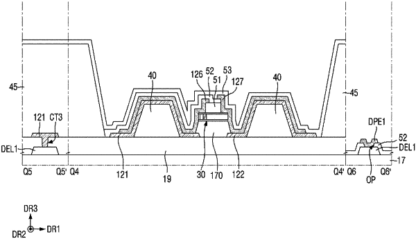
1. A display device comprising:
a first substrate comprising a display area and a non-display area;
first banks spaced apart from each other in the display area and in the non-display area on the first substrate;
electrodes spaced apart from each other on the first banks in the display area;
dummy electrodes spaced apart from each other on the first banks in the non-display area;
a first pattern between the electrodes in the display area;
a second pattern between the dummy electrodes in the non-display area;
a first light emitting element on the first pattern;
a second light emitting element on the second pattern;
contact electrodes respectively on the electrodes in the display area to contact one end of the first light emitting element; and
dummy contact electrodes respectively on the dummy electrodes in the non-display area to contact one end of the second light emitting element.
|