| CPC H10K 59/122 (2023.02) [H10K 50/844 (2023.02); H10K 50/865 (2023.02); H10K 59/38 (2023.02); H10K 71/00 (2023.02); H10K 71/135 (2023.02); H10K 71/211 (2023.02); H10K 71/233 (2023.02); H10K 71/40 (2023.02); H10K 59/1201 (2023.02)] | 15 Claims |
|
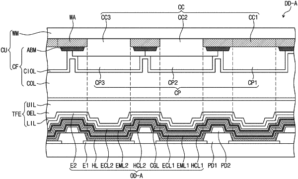
1. A display device, comprising:
a circuit device layer comprising a transistor;
a display element layer comprising:
a first electrode connected to the transistor;
a second electrode disposed on the first electrode;
an organic light emitting layer disposed between the first electrode and the second electrode;
a hole control layer disposed between the first electrode and the organic light emitting layer;
a first layer comprising a first opening exposing the first electrode; and
a second layer disposed on the first layer, the second layer comprising a second opening overlapping the first opening; and
an encapsulation layer disposed on the display element layer,
wherein:
a top surface of the first layer is exposed by the hole control layer and the second layer;
the hole control layer is in contact with the first electrode;
the second electrode is in contact with the top surface of the first layer and a side surface of the second layer defining the second opening; and
the first layer and the second layer contain a same liquid-repellent material.
|