| CPC H10K 59/1216 (2023.02) [G09G 3/3225 (2013.01); H10K 59/126 (2023.02); H10K 59/1213 (2023.02); H10K 59/131 (2023.02); G09G 2300/0426 (2013.01); G09G 2320/0233 (2013.01); G09G 2320/0242 (2013.01); H01L 27/1255 (2013.01)] | 10 Claims |
|
1. A display device comprising:
a substrate;
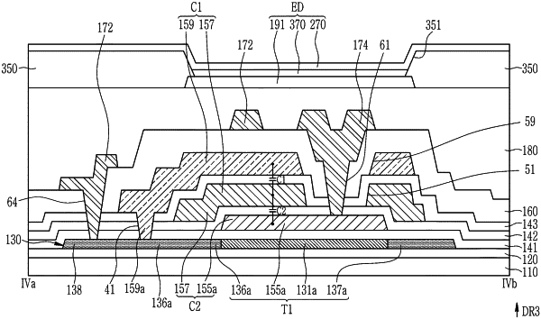
a first transistor disposed on the substrate, the first transistor including a channel region, a gate electrode, a first electrode electrically connected to a driving voltage line, and a second electrode;
a second transistor including a gate electrode, a first electrode electrically connected to the second electrode of the first transistor, and a second electrode electrically connected to the gate electrode of the first transistor;
a third transistor including a gate electrode electrically connected to a first scan line, a first electrode electrically connected to a data line, and a second electrode electrically connected to a first node;
a fifth transistor including a gate electrode electrically connected to a second scan line, a first electrode electrically connected to the first node, and a second electrode electrically connected to the driving voltage line;
a first capacitor including a first terminal electrically connected to the first node, and a second terminal electrically connected to the driving voltage line; and
a second capacitor including a first terminal electrically connected to the gate electrode of the first transistor, and a second terminal electrically connected to the first node,
wherein the first capacitor and the second capacitor overlap the first transistor in a plan view, and
the first capacitor and the second capacitor overlap each other over the first transistor in the plan view.
|