| CPC H10K 50/86 (2023.02) [H10K 50/8428 (2023.02); H10K 59/122 (2023.02); H10K 59/131 (2023.02); H10K 59/121 (2023.02); H10K 2102/351 (2023.02)] | 8 Claims |
|
1. An electronic panel, comprising:
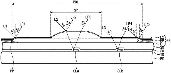
a base substrate including a front surface, a rear surface opposite to the front surface, and a plurality of side surfaces connecting the front surface and the rear surface to each other;
a pixel definition layer on the front surface of the base substrate and having a plurality of openings defined therein;
a plurality of emitting elements in the openings;
a spacer on the pixel definition layer and spaced apart from the openings, wherein the spacer is configured to control a reflection angle of light incident on the spacer to be different from or less than 30°,
wherein a ratio of a thickness of the pixel definition layer to a sum of thicknesses of the pixel definition layer and the spacer is equal to or less than 0.3; and
a plurality of signal lines between the base substrate and the pixel definition layer, the signal lines being electrically connected to the emitting elements, wherein a first signal line of the signal lines between adjacent openings is within a footprint of the spacer in a plan view and a second signal line of the signal lines between the adjacent openings is outside the footprint of the spacer in the plan view with the first signal line and the second signal line are disposed on a same layer,
wherein the spacer includes a first sidewall extending along a direction inclined at a first angle relative to an extending direction of a first side surface among the side surfaces, when viewed from the front surface, wherein the first angle is in a range of 45°±15° or 135°±15°, and
the spacer further includes a second sidewall extending in a direction perpendicular to the extending direction of the first side surface, when viewed from the front surface.
|