| CPC H10K 50/8428 (2023.02) [H10K 50/86 (2023.02); H10K 59/124 (2023.02); H10K 59/131 (2023.02); G06F 3/0412 (2013.01); G06F 3/0446 (2019.05); G06F 2203/04111 (2013.01); H04N 23/57 (2023.01); H10K 59/35 (2023.02)] | 22 Claims |
|
1. A display device comprising:
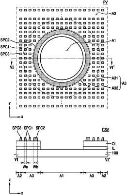
a first substrate comprising a transmission area, a display area surrounding at least a portion of the transmission area, and a first non-display area located between the transmission area and the display area;
an insulating layer arranged on the first substrate in the display area and the first non-display area;
a plurality of display elements disposed on the insulating layer in the display area;
a plurality of first spacers each having an island shape and spaced apart from each other on the insulating layer in the first non-display area, the plurality of first spacers being arranged at intervals in a first direction or a second direction in a plan view; and
a second substrate facing the first substrate.
|